
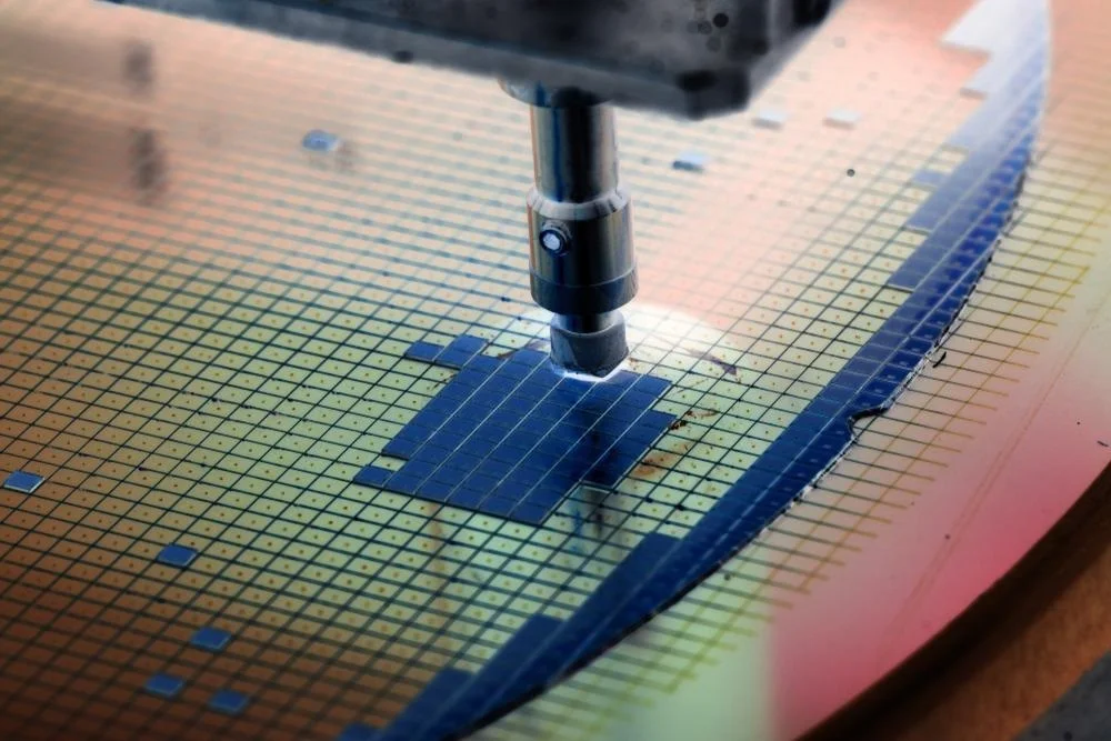
Wafer-level packaging is where a die is packaged while still in wafer form, either single or combined with additional dies or other components such as discrete passive devices or functional features like microelectromechanical systems (MEMS) or radio-frequency (RF) filters. It allows the production of wafer- and panel-level packaging using heterogeneous integration.
Although, by definition, WLPs have historically been produced using either a 200mm or 300mm diameter round wafer format, multiple suppliers are extending similar manufacturing methods to rectangular panel formats. For more details, visit https://www.silybwafers.com/
This process allows the manufacture of heterogeneous packages not only on a wafer-level infrastructure (Wafer Level Packages, or WLPs) but also based on a panel-level infrastructure (Panel Level Packages, or PLPs).
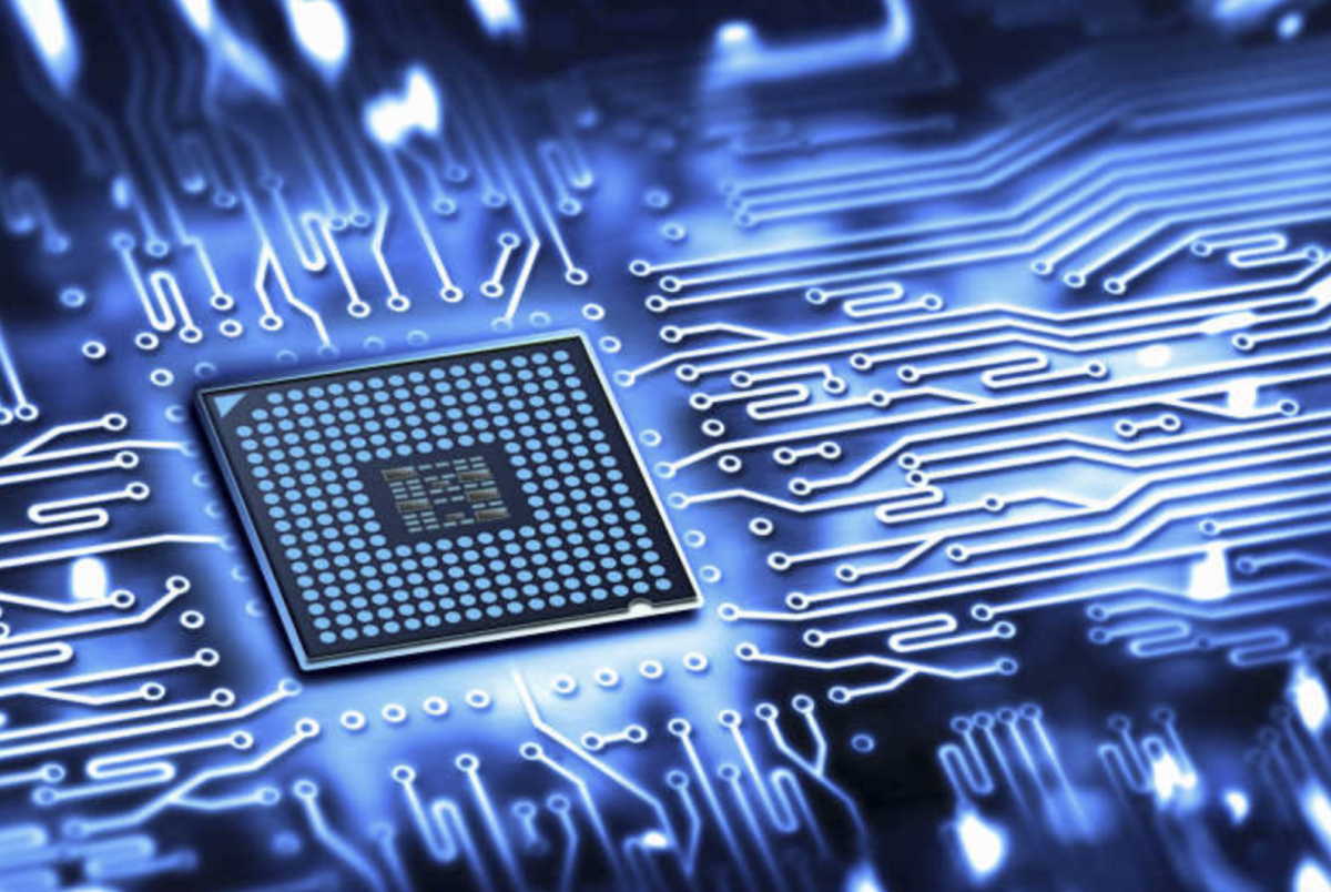
Understanding Wafer Level Packaging And Its Types
WLP is a technology in which all the IC packaging process steps are performed while the devices are still in a wafer structure before singulation. The original WLP designs required that all package I/O terminals be continuously located within the chip outline, producing a valid chip-size package. The system constituted a fan-in Wafer Level Package with the sequential processing of a complete silicon wafer.
1. Wafer Level Chip Scale Packaging (WLCSP)
Wafer Level Chip Scale Packaging (WLCSP) came into its own around 2000 and has been mostly limited to single-die packaging. By the nature of the package, WLCSPs have limited capability to integrate multiple components. Before that time, most packaging processes were mechanical, such as grinding, sawing, wire-bonding, etc. The packaging process steps were performed predominantly after die singulation.
WLCSP was a natural extension of wafer bumping, which IBM had used since the 1960s. The primary difference was the use of large solder balls at a coarser pitch than used for traditional bumped die. Unlike previous packaging, nearly all the WLCSP packaging process steps are done in parallel while still in wafer form.
With WLCSP, since the die becomes the package, it is the smallest package that can be manufactured. Because of its size reduction capability, it has become widely used for small mobile applications. The earliest versions were simply solder balls placed on special “Under Bump Metallization” (UBM) that renders the die pad solderable.
However, as the complexity of the devices increased, it became necessary to add metal redistribution trace layers to route the solder balls away from their respective pads. These redistribution layers (RDL) became the norm, with WLPs increasing in size and complexity.
2. Fan-out Wafer And Panel Level Packaging
While advances have been made in WLCSP and high adoption of such packages for SiPs have been observed in the industry, the boxes are still limited in physical area to the actual die size. As wafer nodes advance, with geometries shrinking, the die themselves could be reduced, bringing more challenges to this package type.
It created a dilemma – where to place the solder balls at the coarser pitch required for WLCSPs. To address this requirement, the “Fan-Out” packaging platform had been conceptualized and was in various stages of development as early as 1983; however, it went into volume production much later, in May of 2009, with the Infineon eWLB product.
The first two primary commercial contenders were Motorola/Freescale with their Reconstituted Chip Package. (RCP) technology, and Infineon developed the above-mentioned embedded Wafer Level BGA (eWLB) technology.
Technologies Used In Wafer Processing Of Semi-Conductors

There are a few essential technologies used in the wafer processing of semiconductors. Here are the same.
1. RCP Technology
The RCP included a copper frame layer embedded in the mold compound and the die, acting as a potential ground plane and a stabilizer for alleviating TCE mismatch to the printed circuit board after final assembly. While RCP seemed to perform better in preventing die shift, it had limited adoption in the market.
It was a technology developed earlier; however, it took until 2011 to make it into manufacturing. NXP was the first to bring RCP to manufacturing for its 77GHz radar applications in collaboration with Nepes.
2. eWLB Technology
Infineon took eWLB into volume production in early 2009. Both processes were an
extension of standard Wafer Chip Scale Packaging (WLCSP) processing technology, with the “wafer level” processing performed on a plastic, reconstituted wafer instead of the traditional silicon wafer. The die was first formed and embedded in a mold compound on five sides, exposing the die pad side.
The molded “reconstituted” wafer was then processed similarly to WLCSPs, with modifications to the materials, equipment, and processes to accommodate the mold wafer’s variability. eWLB had the advantage of having a more straightforward process flow due to fewer process steps, a reason why it had a higher adoption in the market.
Although Casio described their EWLP package as a “Fan In/Out Package” in 2006 [21], the term was not generally used to describe a reconstituted wafer package until Infineon began telling their eWLB package as “Fan-Out WLB.” The time “Fan Out” has gained widespread acceptance in the packaging industry. In their patent for the eWLB technology, Infineon described all previous packaging in this way:
“Conventional packages or casings for circuit units are therefore constructed using a so-called ‘fan-out design.” The only package that does not “fan out” the interconnections is a die-sized WLCSP, which can only fan inward.
The eWLB and RCP fan-out packages were processed as a chip-first structure. The die was molded into a reconstituted “plastic wafer” before the interconnecting trace redistribution layer (RDL) was added to the device. eWLB and RCP can be classified as “die down” chip-first processes, as the die is placed on the temporary carrier before over-molding in a die-face-down position.
Conclusion
The world of technology is an ever-expanding part of our daily lives. Over the past decades, you have seen significant innovations in the semiconductor industry, which significantly impacted our daily activities – from computing and the internet to the introduction of mobile devices and the evolution of smartphones.
While mobile applications have driven a lot of innovation in packaging and semiconductors for the past decade, with strong adoption of wafer-level packaging technologies, new applications are emerging that bring new challenges and requirements across the entire supply chain.
The semiconductor industry is experiencing unprecedented growth across all the different market segments, with new applications such as autonomous driving, 5G, the Internet of Things (IoT), artificial intelligence, machine learning, etc., growing and bringing new opportunities for innovation.


